| ChinAfrica |
| From Simple Link to Whole Chain |
| China’s compound semiconductor industry is surging ahead towards a future of more advanced technology, greater independence and improved security |
| Zhao Yang | VOL. 18 November 2026 ·2026-11-04 |
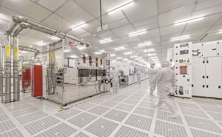
Staff members working in JFS Laboratory (COURTESY)
Engineers dressed in white dust-proof suits move around quietly, busy with debugging and verification work at the JFS Laboratory in China (Hubei) Pilot Free Trade Zone Wuhan Area, also known as the Wuhan Optics Valley.
Armed with an impressive array of the world’s most sophisticated equipment and high-precision testing devices, this facility focuses on research into compound semiconductors. Currently, more than 100 research projects are underway here, each holding the potential to spark the next industrial revolution.
In recent years, continuous breakthroughs have been made in chip technologies in Optics Valley, where a large number of sci-tech companies, including Huagong Tech Co. Ltd., are concentrated, alongside the world’s largest research and pilot-scale testing platforms for compound semiconductors. Their combined efforts are helping China’s semiconductor industry make steady progress and upgrade at an unprecedented rate.
Breakthroughs at enterprises
“This stealth dicing equipment can cut wafers thinner than human hair, and it has reached an internationally advanced level for indicators such as cutting precision and edge chipping control,” Huang Wei, general manager of the semiconductor product line, told China Today when explaining Huagong Tech’s high-end laser equipment manufacturing workshop. This equipment is not only the company’s flagship product, but also a prime example of China’s independent innovation in key semiconductor technology.
Over recent years, intensifying global technological competition has profoundly affected the security and stability of the semiconductor supply chain. Facing restrictions on imports of high-end equipment, China has accelerated localised production. “Laser dicing is a crucial part of wafer manufacturing and directly affects wafer yield and cost,” Huang said. Before a new piece of equipment enters the market, it needs to undergo repeated testing and verification in a real production environment. This is a lengthy cycle that carries great risks and makes advancement very difficult.
To tackle this problem, Huagong Tech, together with the Huazhong University of Science and Technology, the JFS Laboratory and other organisations, established a joint innovation laboratory. With Huagong Tech leading the equipment research and software algorithms at the JFS Laboratory, researchers collaborated to simulate an authentic production environment and completed over 1,000 hours of pilot-scale testing for the first-generation equipment in six months.
At the end of this process, the equipment’s precision and reliability reached optimal levels, and it received a verification report issued by the JFS Laboratory clearing it for use on production lines. It became China’s first high-end wafer laser dicing equipment with all core components domestically produced, providing solid support for the country’s endeavour to achieve independence in the production of semiconductor equipment.
“At the JFS Laboratory, research, development and verification proceed in parallel, shortening the process by at least half. The qualification certification also gives customers more confidence in domestic equipment. This helps with our independent development of laser annealing equipment for silicon carbide wafers,” Huang said.
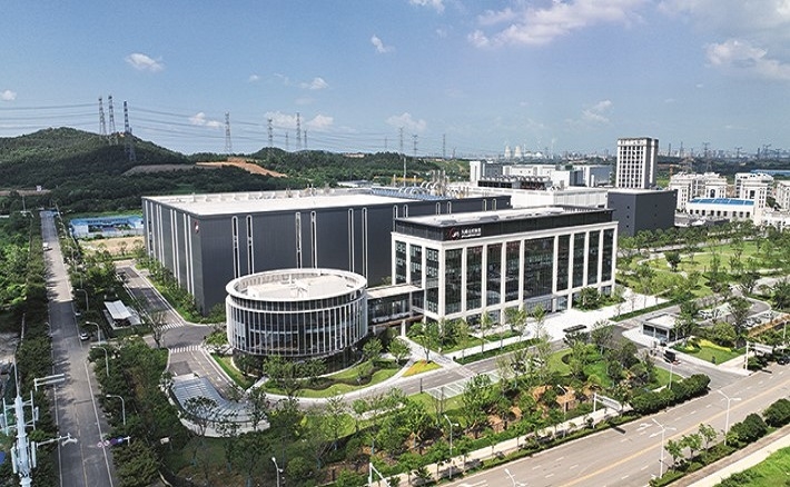
A view of JFS Laboratory (COURTESY)
Guiding role of national platforms
Founded in 1999 by the Huazhong University of Science and Technology, Huagong Tech has demonstrated astonishing capacity to evolve. Driven by its three major businesses - optical interconnection, intelligent sensing and intelligent manufacturing - the company has built a symbiotic industrial ecosystem that supports win-win cooperation. Upstream, it focuses on core materials and key components to ensure the independence of the industrial chain; downstream, it opens up application scenarios and collaborates with leading customers in fields such as shipbuilding and new energy to create national-level demonstration projects for smart factories, which in turn drive further advances in upstream technologies.
Over the past decade, Huagong Tech has not only achieved independence in the production of high-end laser equipment, but also maintained an annual growth rate of 35 percent in global sales of its core products.
A single enterprise’s advancement, however, is not enough to lift the entire industry out of its predicament. The JFS Laboratory has therefore become a development “booster” for many compound semiconductor enterprises and research institutions.
The laboratory’s exhibition area displays samples ranging from raw materials to finished products: crystal-clear gallium oxide ingots, 12-inch silicon carbide substrates and fingernail-sized chips that reveal, under a microscope, layers as densely packed as a metropolis. Together, they showcase one of the industry’s most in-demand technologies: compound semiconductors.
According to Wu Chang, head of the research department at the JFS Laboratory, compound semiconductor materials, known for their high-frequency, high-power and high-temperature resistance characteristics, are widely used in fields such as new-energy vehicles, 5G communications and photovoltaic power storage. They are key to China’s efforts to achieve self-sufficiency in critical materials and chips. Indium phosphide, for example, has become one of the best options for balancing technology and cost in high-speed optical interconnections at AI data centres.
“Good ideas and good technologies must ultimately move from paper to products. Pilot-scale testing can be a major hurdle on the road to mass production,” Wu said. The JFS Laboratory serves as a vital experimental field that brings together extensive equipment and innovation resources.
Every piece of work carried out at the JFS Laboratory contributes to the improvement and upgrading of the compound semiconductor industrial chain. At the end of 2025, the laboratory was selected as part of the first batch of national-level manufacturing pilot-scale testing platforms, the only one in its field.
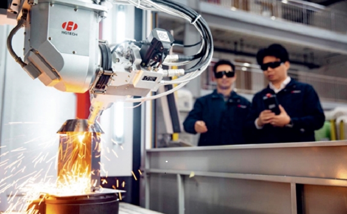
Huagong Tech’s high-end laser equipment (COURTESY)
Collaboration across the basin
If the JFS Laboratory is a lighthouse illuminating the way ahead, the industrial ecosystem cultivated by Optics Valley over decades is the solid foundation that supports this lighthouse.
Since the 1980s, Optics Valley has cultivated a robust optoelectronic industry, building a self-supporting industrial chain with close collaboration among all parties along it. “In Optics Valley, it takes only 20 km to complete the optoelectronic industry chain. For laser equipment manufacturing, suppliers can be reached within a 10-km radius and deliver their products within an hour,” said a manager of Huagong Tech.
This region-wide symbiotic innovation ecosystem greatly reduces logistics and communication costs, making collaboration among enterprises as convenient as visits among neighbours. More importantly, the government provides systematic support, ranging from tax deductions to special industrial funds. The confluence of universities, research institutes and enterprises also creates a large pool of talent.
This innovation ecosystem generates a chain effect that strengthens the industrial chain both upstream and downstream and extends along the Yangtze River waterway.
Optics Valley’s appeal as a global innovation hub for compound semiconductors was evident at the 2026 JFS Forum, held in April in Wuhan. The event set new records, with more than 1,000 technologies unveiled and 35,000 participants.
| About Us | Contact Us | Advertise with Us | Subscribe |
| Copyright Beijing Review All rights reserved 京ICP备08005356号-5 京公网安备110102005860号 |


